

How to run AI workloads on mixed GPUs quickly and affordably

News
Kim Martineau
Today's AI is ubiquitous—from voice assistants to image recognition, process automation and so much more. It’s all thanks to ever more mature algorithms, large amount of training data, and record computer performance. But as tasks become more complex, requiring deployment flexibility and fast execution, continuing the use of conventional processors is simply not scalable. Take energy consumption: training the most advanced AI models has required exponentially growing compute resources, roughly doubling every three months, yielding a sizable carbon footprint.
This is where the IBM Research AI Hardware Center comes in. With 16 leading companies and universities as members, the Center aims to drive technology innovation towards more efficient and sustainable AI.
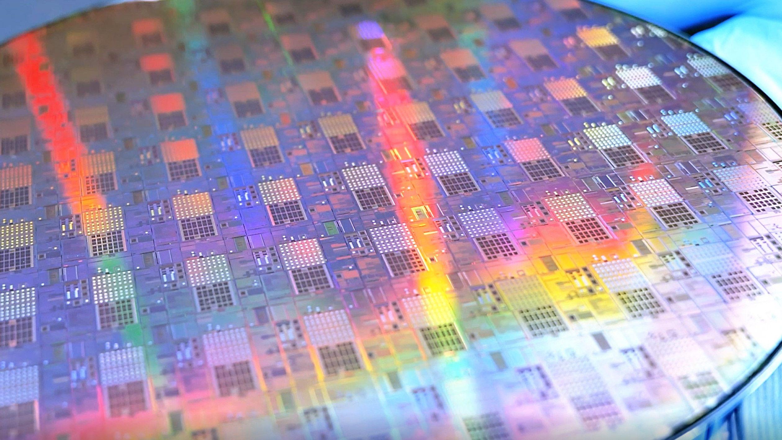
And in June 2021, it unveiled a new chip packaging technology1 at the IEEE ECTC conference, and a first in analog compute2, 3 at the VLSI Technology and Circuits Symposia.
With DBHi, or Direct Bonded Heterogeneous Integration, a silicon communication bridge directly connects neighboring processing chips to enable the high-bandwidth, low-latency, and low-power data transfer required by AI workloads. While this innovation can help scale the efficiency of IBM's digital accelerators, the Center is also exploring analog computation that promises significant additional performance benefits.
In a major leap forward, the synaptic weights of deep neural networks were mapped to millions of non-volatile analog elements, built by IBM on top of a 14-nanometer node front-end technology, and fully on-hardware recognition tasks were performed with promising accuracy.
Since its founding, the IBM Research AI Hardware Center has delivered at least one compute core annually, while maintaining a performance improvement target of 2.5x per year. Most notably, the 2021 IBM digital AI core outperformed that metric and set new records, surpassing commercial offerings of market leaders.
At the heart of this disruptive hardware technology is the understanding that the precision needed to train and run AI can be relaxed. In other words, some degree of fuzziness can be tolerated without affecting the accuracy of the results—provided the AI algorithms are carefully co-optimized. This means needing fewer digital bits to represent a given value, in turn decreasing the size of logic circuits used to perform a calculation.
The scaling and energy benefits are exponential. When the precision is halved, the chip area needed for compute is reduced by a factor of four. While most machines operate today at 64-bit, the latest IBM core architecture built on 7-nanometer extreme-ultraviolet (EUV) technology can handle reduced-precision data types down to 8-bit floating-point and 2-bit fixed-point.4 That’s applicable to a variety of networks and workloads, such as natural language processing and image classification.
The performance capabilities are scalable with the number of chips, highlighting the reliance on advanced packaging techniques to further expand both compute and memory capacity. Indeed, ever-growing models demand large data consumption in AI workloads, so much so that data movement between memory and compute units restrict the performance of accelerators. The ability to package multiple chips with 2D and 3D low-latency high-bandwidth connections promises to enable more efficient specialized hardware with load-balanced compute and memory elements assembled from a set of standard and optimized building blocks.
Together with precision scaling, the IBM Research AI Hardware Center is also pushing boundaries of multi-chip and chiplet packaging in lateral and vertical dimensions.
It just announced at IEEE ECTC the new DBHi technology1 that uses silicon as a communication bridge bonded between chips with copper pillars. That's not all. The Center also reported for the first time on other advances made in packaging technologies, including advanced laminates, 3D integration (3Di), hybrid bonding, photonics, advances in thermal management, and AI-enabled modeling for packaging applications.
As a show of confidence in the future of the packaging technology, IBM is making significant investments in partnership with NY CREATES at our Albany, New York research site to further expand on the capabilities and scope of our advanced heterogeneous integration agenda.
Even beyond the impressive capabilities of digital reduced-precision AI compute cores and their scalability potential with 2D and 3D packaging, the broad innovation horizon of the IBM Research AI Hardware Center roadmap extends to novel analog AI architectures. Neural networks are mapped onto arrays of non-volatile memory (NVM) elements acting as synaptic weights. Multiplication and addition operations are performed in-place, largely eliminating costly data movement, promising unparalleled speedup and energy efficiency for AI workloads.
In June 2021, the IBM Research AI Hardware Center reached a significant milestone and announced a world first 14-nanometer fully on-hardware deep learning inference technology. It is used not in one but two types of analog AI compute chips based on back-end inserted Phase Change Memory (PCM).
On one hand, an all-analog chip2 relies on 35 million PCM devices and time-encoded communication to perform end-to-end multi-layer neural network inference with 8.9 million synaptic weights without extensive use of analog-to-digital converters (ADCs).
Benchmarking on the common Modified National Institute of Standards and Technology (MNIST) image datasets yields classification with good accuracy. On the other hand, a mixed-precision analog chip3 demonstrates inference on MNIST actually matching digital accuracy, while scalability to large neural nets is evidenced by a ResNet-9 network, running at 85.6% classification accuracy on the CIFAR-10 dataset at record speed (10.5 TOPs per Watt and 1.6 TOPs per square millimeter).
Details on the design and performance of the two chips are described in papers, selected as highlights in the 2021 IEEE VLSI Technology and Circuits Symposia.
While the IBM AI Research Center team continues to address in-memory compute challenges towards iso-accuracy in large networks at record efficiency, everyone can now use the IBM Analog Hardware Acceleration Toolkit to simulate both inference and training within the artificial synaptic arrays.5
A no-code-required experience version of the toolkit can be accesses via the AI Hardware Composer, which comes with pre-defined presets users can choose from to build their network.
Precision scaling, advanced chiplet packaging and in-memory computing constitute the foundation needed to optimize data movement and maximize throughput. The IBM Research AI Hardware Center will continue to meet the AI technology challenges and sustain its innovation pace by combining some or all of these elements in its upcoming cores.
Foundational Hardware Technology: At IBM Research, we’re working on semiconductor innovations for the hybrid cloud and AI — foundational hardware technology that we can use to build the next generation of chips to solve those challenges.
Sikka, K., Divakaruni, R., et al. "Direct Bonded Heterogeneous Integration (DBHi) Si Bridge". 2021 IEEE 71st Electronic Component and Technology Conference (ECTC), Proceedings, p. 136 ↩ ↩2
Narayanan, P., Burr, G. W., et al. "Fully on-chip MAC at 14nm enabled by accurate row-wise programming of PCM-based weights and parallel vector-transport in duration-format". 2021 Symposium on VLSI Technology, Digest of Technical Papers, T13-3 ↩ ↩2
Khaddam-Aljameh, R., Eleftheriou, E., et al. "A 14nm CMOS and PCM-based In-Memory Compute Core using an array of 300ps/LSB Linearized CCO-based ADCs and local digital processing". 2021 Symposium on VLSI Technology, Digest of Technical Papers, JFS2-5 ↩ ↩2
Venkataramani, S., Gopalakrishnan, K., et al. AI Accelerator for Ultra-low Precision Training and Inference. 2021 ACM/IEEE 48th Annual International Symposium on Computer Architecture (ISCA). (2021). ↩
Rasch, M. J., Narayanan, V., et al. "A Flexible and Fast PyTorch Toolkit for Simulating Training and Inference on Analog Crossbar Arrays". 2021 IEEE 3rd International Conference on Artificial Intelligence Circuits and Systems (AICAS), Proceedings. (2021). ↩


