National Academy of Engineering recognizes T.C. Chen’s role in semiconductor evolution
Q & A
Peter Hess
IBM Research, in partnership with our Albany Research Alliance partner Samsung, has come up with a breakthrough in semiconductor design — called VTFET — that could help reshape the semiconductor industry for years to come.
IBM Research, in partnership with our Albany Research Alliance partner Samsung, has come up with a breakthrough in semiconductor design — called VTFET — that could help reshape the semiconductor industry for years to come.
Back in 1965, computer scientist Gordon Moore first hypothesized that the number of transistors and other components in a dense integrated circuit would double as well as double the speed and capacity of computers, roughly every two years. But over 55 years later, the number of transistors that can be crammed onto a single chip has just about reached its limit.
At the same time, the road ahead for computing systems isn’t slowing down. Dynamic AI systems are poised to supercharge so many aspects of our lives — from road safety to drug discovery and advanced manufacturing — which will require considerably more powerful chips in the future. In order to continue the advances in speed and computing power that Moore posited, we’ll need to build chips with as many as 100 billion transistors.
IBM Research, in collaboration with our Albany Research Alliance partner Samsung, has made a breakthrough in semiconductor design: Our new approach, called Vertical-Transport Nanosheet Field Effect Transistor, or VTFET, could help keep Moore’s Law alive for years to come.
Today’s dominant chip architectures are lateral-transport field effect transistors (FETs), such as fin field effect transistor, or finFET (which got its name because silicon body resembles the back fin of a fish), which layers transistors along a wafer’s surface. VTFET, on the other hand, layers transistors perpendicular to the silicon wafer and directs current flow vertical to the wafer surface. This new approach addresses scaling barriers by relaxing physical constraints on transistor gate length, spacer thickness, and contact size so that these features can each be optimized; either for performance or energy consumption.
With VTFET, we’ve managed to successfully demonstrate that it’s possible to explore scaling beyond nanosheet technology in CMOS semiconductor design. At these advanced nodes, VTFET could be used to provide two times the performance or up to 85 percent reduction in energy use compared to the scaled finFET alternative.1
The new VTFET architecture demonstrates a path to continue scaling beyond nanosheet. In May, we announced a 2-nanometer node chip designs which will allow a chip to fit up to 50 billion transistors in a space the size of a fingernail. VTFET continues the innovation journey, and opens the door to new possibilities.
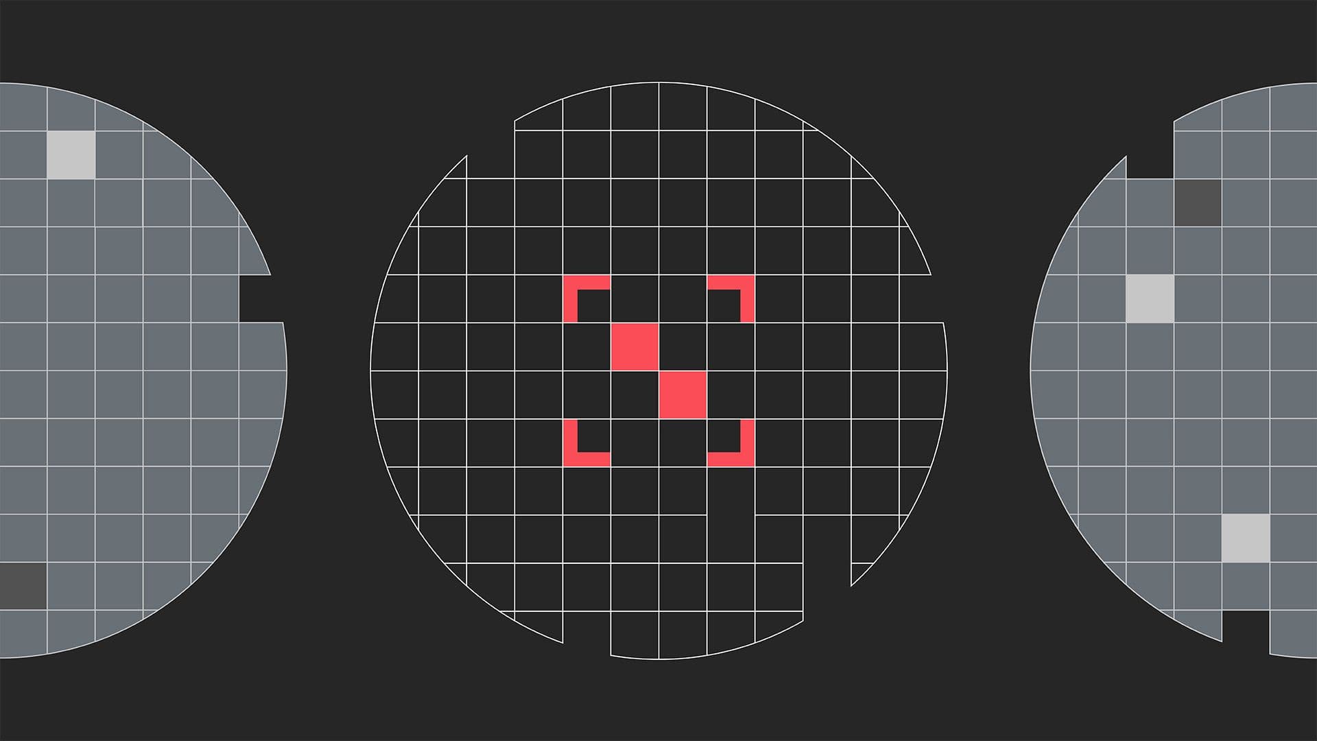
In the past, designers packed more transistors onto a chip by shrinking its gate pitch and wiring pitch. The physical space where all the components fit is called the Contacted Gate Pitch (CGP). The ability to shrink gate and wiring pitches has allowed integrated-circuit designers to go from thousands to millions to billions of transistors in our devices. But with the most advanced finFET technologies, there’s only so much room for spacers, gates and contacts. Once you’ve reached the CGP limit, you’re out of space.
By orienting electrical current flow vertically, the gates, spaces and contacts are no longer constrained in traditional ways: We have room to scale CGP while maintaining healthy transistor, contact, and isolation (spacer and shallow trench isolation, STI) size. Released from the constraints of the lateral layout and current flow, we were able to use larger source/drain contacts to increase the current on the device. The gate length can be selected to optimize device drive current and leakage, while the spacer thickness can be independently optimized for lower capacitance. We are no longer forced to tradeoff the gate, spacer, and contact size, which can result in improved switching speed and reduced power use.
Another key VTFET feature is the ability to use STI for adjacent circuit isolation to achieve a Zero-Diffusion Break (ZDB) isolation, with no loss of active-gate pitches. By comparison, the density of lateral-transport FET circuitry is affected by double or single-diffusion breaks required for circuit isolation, which affects the ability to further shrink the technology.
Even a decade ago, we could see lateral architectures would hit scaling limits at aggressive gate pitches: practically, each of the device components were nearing scaling limits. We wanted to find other paths that could break those barriers, and our motivation has never changed. Our goal has always been to produce a competitive device for the technologies of the future.
With a gate pitch more aggressive than anything known in production and CMOS logic transistors at sub-45 nm gate pitch on bulk silicon wafers, we believe that the VTFET design represents a huge leap forward toward building next-generation transistors that will enable a trend of smaller, more powerful and energy-efficient devices in the years to come.
Semiconductors: Semiconductors power every electronic device, from smartphones to medical equipment. With advances in research, these devices have become smaller, faster and more reliable.
VTFET nanosheet and scaled finFET device simulation results are compared at the same footprint and at an aggressive sub-45nm gate pitch. VTFET nanosheets provides ~ 2X performance of the scaled finFET at equivalent power due to VTFET maintaining good electrostatics and parasitics while finFET performance is impacted by severe scaling constraints. Or VTFET could provide as much as 85% power reduction compared to the scaled finFET architecture as compared at an equivalent frequency on the extrapolated power-performance curves. ↩