IBM, Canada, and Quebec are partnering to secure the future of chipmaking in North America
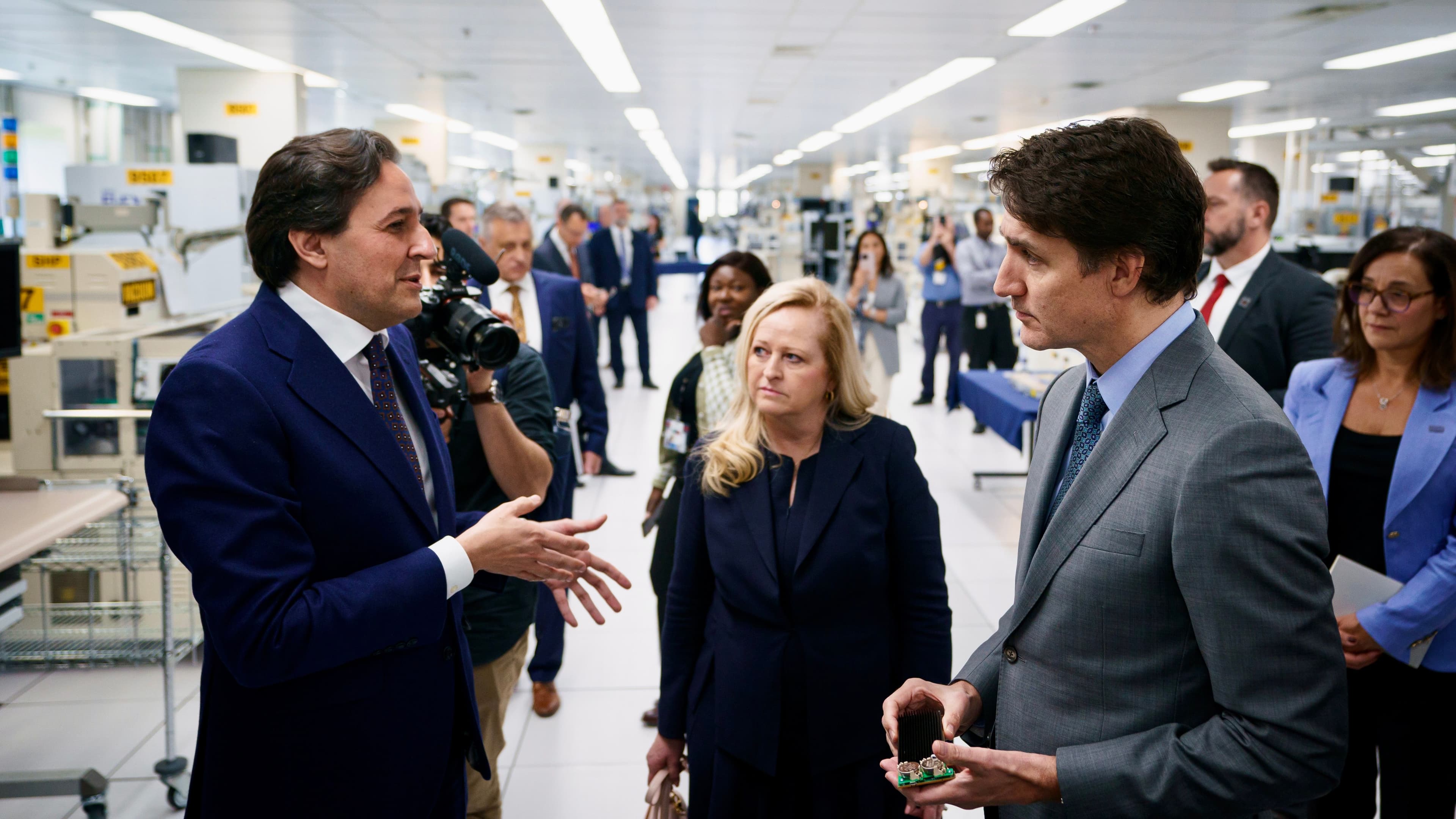
As demand for chips continues to surge from AI and cloud computing advances, the Canadian and Quebec governments are partnering with IBM to solidify the future of the chip supply chain in North America by advancing the assembly, testing, and packaging capabilities at IBM's plant in Bromont, Quebec.
Nestled in the hills of southern Quebec sits a facility that operates 24 hours a day, every day of the year, building over 100,000 microelectronic devices each week.
These chips are devices that have been packaged up by the team at the IBM Canada plant in Bromont, one of the largest chip research and production facilities in North America.
The world is experiencing an explosion in demand for computer chips. Consumer devices are becoming ever smaller and more complicated, more and more businesses are moving to the cloud, and the demand for AI processing power is increasing exponentially. These days, the vast majority of the chips produced in the world are made in the East. But the pandemic made it clear that demand is growing faster than ships can send chips around the world, and many countries are looking to bring chip production closer to home.
That’s why at an event today at IBM Canada plant in Bromont, the government of Canada, IBM, and the government of Quebec announced an agreement to deepen the capabilities of the facility. Among the three entities, they will invest up to CA$187 million in advancing the assembly, testing, and packaging capabilities at the plant in Bromont. This will enable IBM to further its research and development of methods for scalable manufacturing and other advanced assembly processes. “Semiconductors power the world, and we’re putting Canada at the forefront of that opportunity,” said Canadian Prime Minister Justin Trudeau.
When it comes to computer chip innovations, we often think about how to cram more silicon transistors into increasingly small spaces. IBM Research has been at the forefront of semiconductor research more or less since the invention of the field, and continues to push the industry forward with advances in 2 nanometer-node chips, and beyond. But equally important in the chip manufacturing process is how these devices are packaged up so that they can be installed in groundbreaking products, like smartphones, cars, IBM Z systems, wearables, and AI cloud servers — just about any modern device with a processor in it.
Designing the packages for chips, as well as the tooling and assembly logistics for building them at scale, is a major part of what the IBM research and development team at IBM Canada’s Bromont plant does every day. With this new investment, they will be able to scale up their production work like never before.
Beyond scaling packaging work, the investment will also allow researchers to explore how to package different chip technologies, such as chiplets. These are computing parts that can connect to others to form new powerful processing devices — such as a system designed for AI inferencing that might have considerably more memory onboard than a traditional CPU would. Many argue that these sorts of devices will be crucial to support the demand of the Cambrian explosion we’ve seen in AI in recent years.
This investment could help shape the North American semiconductor supply chain of the future, and ensure that Canada does not have to rely only on manufacturing and design partners that are based thousands of miles away for their chips. The agreement also allows for collaborations with small- and medium-sized businesses from Canada, with the intent of fostering the development of a semiconductor ecosystem in the country.
At IBM Bromont, device module packaging and testing is currently offered for a wide range of clients, including IBM — the facility packages the chips used in IBM’s Z and P systems. It also happens to be the largest Outsourced Semiconductor Assembly and Test (OSAT) facility in North America, and a US government-trusted facility. Overall, it’s one of North America’s largest chip assembly and testing facilities, and has been in near-constant operation for over 52 years. It’s part of IBM’s full-stack approach to creating the future of chips, with research facilities exploring the raw materials for tomorrow’s chips, and how they’re fabricated into semiconductors in Albany and Yorktown Heights, New York.
Demand for computing resources has surged as we enter the age of AI, IBM’s Senior Vice President and Director of Research Darío Gil said. But rising to the moment is something IBM Research does. “IBM has long been a leader in semiconductor research and development, pioneering breakthroughs to meet tomorrow’s challenges. said Gil “As one of the largest chip assembly and testing facilities in North America, IBM's Bromont facility will play a central role in this future.”
“We are proud to be working with the governments of Canada and Quebec toward those goals,” Gil added, "To build a stronger and more balanced semiconductor ecosystem in North America and beyond.”
Related posts
- NewsMike Murphy
Here comes a foundation model for the Sun
ReleaseKim Martineau and Mike MurphyTowards a generative future for computing
ReleaseMike MurphyHow the IBM Research AI Hardware Center is building tomorrow’s processors
Deep DivePeter Hess
