


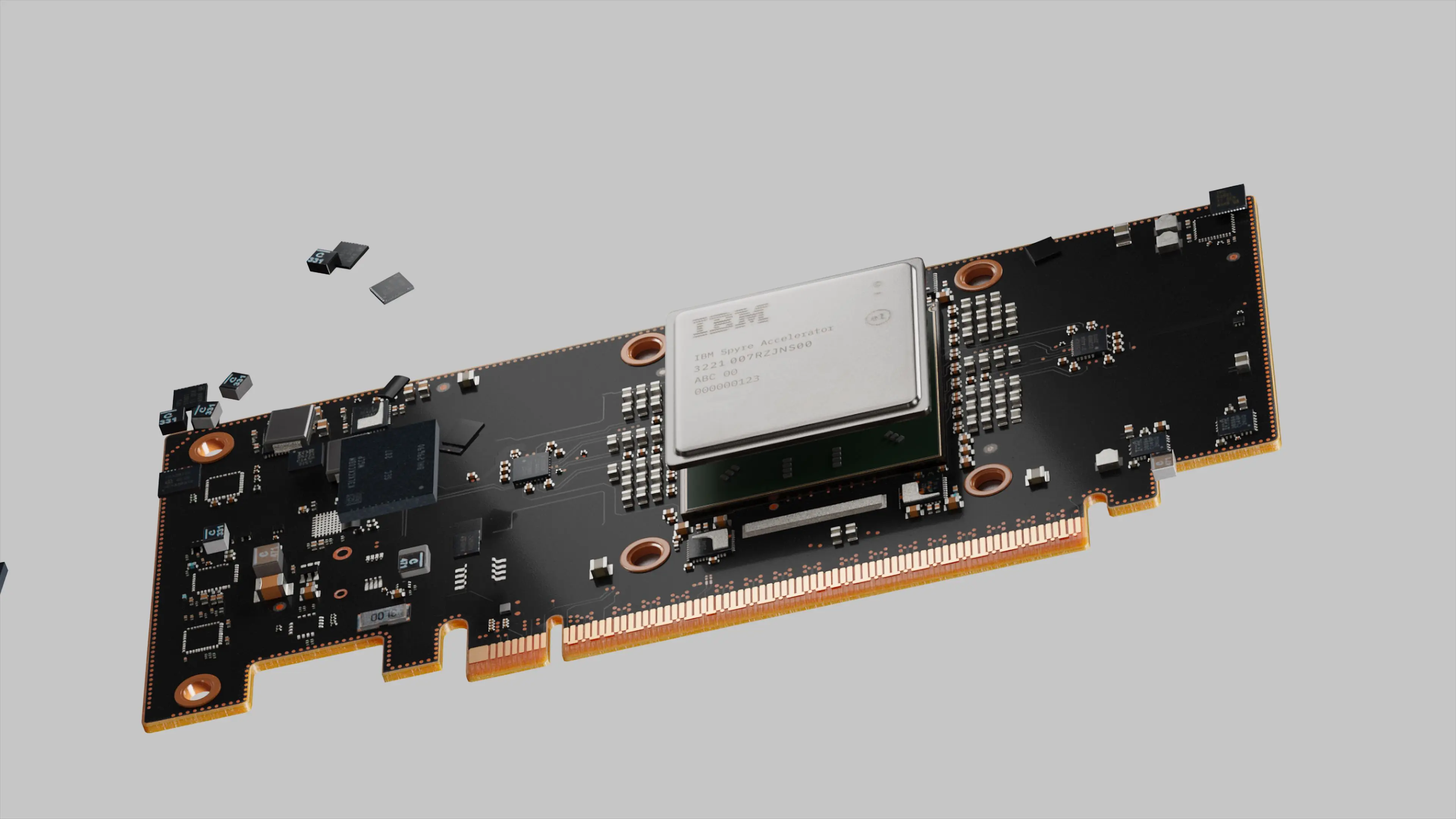
Building the IBM Spyre Accelerator
Release
Peter Hess
After 75 years of dramatic advances, the digital computer is bumping against its limits, constrained by its architecture and atomic physics. To continue making smarter, faster and more efficient machines, systems researchers at IBM are pioneering new technologies and approaches. In this blogpost, the fourth in our series dedicated to Women in IBM Research, we meet four scientists—in Japan, Switzerland, California and New York. They’re working to transform computing with AI hardware accelerators, nanosheet technology, and spintronics. The goal is not simply to make smarter machines, but to create deep-learning platforms that help solve our most pressing and intractable problems.
AI hardware accelerators have become a popular area of systems research as chipmakers look for ways to speed up hardware to better accommodate machine learning and other data-heavy AI workloads.
Hsinyu (Sidney) Tsai , Research Staff Manager, Analog AI for Deep Learning Acceleration, at IBM’s Almaden Research Center, leads a team developing technologies to further boost the performance and efficiency of AI hardware, by addressing a fundamental bottleneck of traditional chip architectures. It was in 1945 that the mathematician John von Neumann mapped out the future digital machines, and separated memory from processing. Ever since, computers have had to shuttle data back and forth between those two functions. This slows them down and consumes loads of energy. It is known as “the von Neumann bottleneck.”
Tsai and her IBM Research colleagues are developing an analog-based accelerator that can better accommodate deep learning’s matrix vector multiplication requirements. “Using Von Neumann architectures, you read the matrix you want to compute from memory and load it into some compute unit,” she says. “Then you load the vector and then do the compute.”
The idea behind their analog AI accelerator is to enable vector multiplication in place—where the memory sits—in order to avoid data movement bottlenecks and improve energy efficiency. “Analog AI accelerators are specifically designed to reuse the data as much as possible on the chip and to move things around as infrequently as possible,” she says.
The team’s in-memory AI accelerator work began in 2014. At the time, Tsai had just given birth to her son. “It struck me how similar training deep-learning neural networks was to teaching a child,” says Tsai, who now also has a daughter. “You start with image recognition and then move on to things like language.”
Tsai’s love of math and physics led her to pursue electrical engineering at a young age—students in her native Taiwan are told to pick an area of focus and stick with it throughout much of their schooling. She attended National Taiwan University, double majoring in electrical engineering and physics, before landing at Massachusetts Institute of Technology (MIT), where she earned her Ph.D. in electrical engineering and computer science in 2011. She joined IBM’s T.J. Watson Research Center in Yorktown Heights later that year and in 2015 became Manager of Advanced Lithography Group in the Microelectronics Research Lab.
The following year, she moved to the Bay Area with her family. She knew that the relocation to Almaden would be a departure from her deep expertise in lithography. “I was confident that I could continue to grow my career, even if the trajectory proved decidedly non-linear. It’s been an unusual career path – stepping up to advanced lithography management in Yorktown, stepping out of management to come to work on in-memory computing in Almaden and then in an AI Hardware management role a few years later.”
Her first contact with AI came toward the end of her tenure at MIT, when she attended a thesis defense about using mouse neurons to develop more hierarchical, neuron-based visual models. “I was impressed by the idea of having bio-inspired building blocks and getting 98 percent classification accuracy,” Tsai says. “Of course, it took this person their entire Ph.D. to do this work, because people hadn’t yet started building hardware accelerators to help speed up their research.” Since then, she has been determined to address that shortcoming.
Whereas Tsai is working on the AI chip architecture for Analog AI Hardware, translating an AI model into analog AI hardware involves developing new materials that both store and process data—much the way our brains do—in billions of tiny synapses. Valeria Bragaglia is one of a team IBM Researchers in Zurich Research Lab, creating programmable devices—so-called “artificial synapses”—to encode AI model parameters. To this end, she grows tiny batches of different materials, tuning and testing their electrical and physical properties.
Early work on analog AI hardware has used Phase Change Materials (PCM), in which the microstructure of the PCM can be modulated and the resulting resistance used to encode the neural network “weight”. This approach has fueled rapid progress in Analog AI hardware and demo accessed on the cloud and run directly on a chip in the Zurich lab. Bragaglia and her colleagues are currently focused on modifying material chemistry and microstructure to create the perfect analog material for AI applications.
She sees the potential of this technology to dramatically increase the speed and efficiency of deep neural networks. Analog AI hardware might prove to be the most powerful and efficient tool to pile through ever larger troves of data, deciphering language, recognizing patterns, and reaching more nuanced, and even creative conclusions,” she says.
Bragaglia’s and Tsai’s current work is part of the IBM Research AI Hardware Center , where IBM researchers from Zurich, Tokyo, Almaden, and New York collaborate to combine fundamental advances in AI with new computing accelerators, technologies, and architectures designed and optimized specifically for AI computation.
Born to Italian parents, Bragaglia grew up in Germany and Italy. She went to university in Rome and then moved to Berlin for her PhD. In the beginning of her graduate studies, she focused on experimental physics, developing materials with dedicated properties. She continued with her postdoc at IBM Research, where she was excited to turn her research to applied physics. “It’s a bit between academia and industry,” she says. “It gives you the possibility to work in different fields.”
Bragaglia keeps very busy outside the lab. She plays classical piano and loves to dance, especially Argentine tango. She also paints, both people and abstract landscapes. These days, she says, she does most of her painting in acrylic. It dries faster—giving her more time to her next project, both in the lab and outside of it.
IBM Research has long pushed the limits of semiconductor technology in its quest to develop smaller, faster and more reliable chips. As chip transistor sizes shrink to only a handful of nanometers, however, Indira Seshadri and her team of IBM researchers find themselves in increasingly uncharted territory—seeking new ways to scale below silicon’s 7-nanometer limit .
“Scaling, especially that small, is difficult,” says Seshadri, Technical Lead at IBM Research – Albany. Her team is responsible for investigating and identifying new chip architectures for IBM Systems engineers to build. One of the most promising developments in their lab is stacked gate-all-around Nanosheet structure, which can address logic device needs at 5nm technology nodes and beyond better than the existing fin field-effect transistor ( FinFET ) multi-gate devices that gradually came to dominate the semiconductor market during the previous decade.
“IBM was the first in the industry to demonstrate Nanosheet architecture, whose superior computing performance and lower power consumption will benefit AI systems, mobile phones and a variety of other devices,” she says. “Whoever can do it and be first to market stands to benefit the most.”
The Nanosheet research complements Seshadri’s work developing Extreme Ultraviolet (EUV) lithography, which uses extremely short wavelength EUV light to etch fine circuit patterns into semiconductor wafers. “IBM is helping move the chipmaking industry to EUV, which has come a long way over the past 15 years, to the point where it’s become mainstream,” she says. “Together, Nanosheet architecture and EUV lithography will play a crucial role in scaling down future generations of chips.”
Engineering challenges are nothing new to Seshadri. She grew up in southern India, where her single mother owned a factory that made brake linings—the rough material attached to a brake shoe that increases friction and helps bring your car to a stop. As a child, Seshadri would spend most afternoons after school at the factory. “I was exposed to mechanical engineering at a very young age,” she says. As a fourth-grader, Seshadri would help factory workers inspect parts. “It came as a surprise to me to learn later on that mechanical engineering was not a common profession for women.”
After earning an undergraduate engineering degree in 2006 from the College of Engineering, Guindy at Anna University in Chennai, India, Seshadri continued her education at The Ohio State University. “I was thinking in terms of working in industry as a mechanical engineer, and the [U.S.] Midwest seemed like a good place to find those jobs,” she says.
She earned her master’s mechanical engineering in 2008 but found her first jobs in industry to be fairly repetitive, with more emphasis on cost-cutting and meeting deadlines than innovating. Seshadri wanted to solve new problems and decided she would need to go back to school to put her career on that path. “Once you’re in the workforce, going back to school is a hard decision,” says Seshadri, who was already married at the time. “It’s worth it because it gives you more opportunities.”
Seshadri earned her Ph.D. from Rensselaer Polytechnic Institute in 2014, defending her thesis mere weeks after giving birth to her son. The following year she joined IBM Research in Albany. “What I enjoy most about working here is digging deeper into problems and coming up with solutions,” she says. “We’re often trying to do things that no one else in the world has done.”
As the world of computing extends to trillions of devices, from sensors in rain forests to cameras on the ocean floor, one great challenge looms: How to power the vast Internet of Things (IOT). The hunt for low-power computing has led Akiyo Nomura, a researcher at IBM’s Tokyo labs, to the field of analog AI Hardware research.
Akiyo Nomura joined IBM in 2017 as a researcher in the Neuromorphic Device group. The group is located in the IBM Shin-Kawasaki facility at NANOBIC, a research park owned by Kawasaki City for open innovations in micro/nano technology. Although her major in university was solid-state physics with a focus on spintronics, she was able to begin her research journey at IBM by acquiring IC circuit design skills and knowledge of neural networks. She has been working on a next-generation analog AI hardware accelerator for deep neural networks and spiking neural networks. The accelerator enables in-memory operation by utilizing new synaptic-element devices and circuit technologies. She has presented the results of her research at international conferences, and she has also published her work in journals. She is enjoying working with global IBM researchers to come up with new concepts for AI hardware circuits. Improving all elements such as algorithms, architectures, circuits, and devices will lead to the success of research on analog AI hardware. “It’s all very interesting to explore,” Nomura says.
Nomura grew up in a small town with rich nature, in the Gunma Prefecture, located north of Tokyo. “Trains come only once every 30 minutes,” she says. Always interested in technology, she went to Yokohama to study, and received her master’s degree from Keio University in physics. She joined IBM Research in 2017.
Nomura is married to an engineer, she met at Keio University. In her free time, she says, she enjoys cooking. She makes her own chicken and beef stocks, and specializes in different curries. “The variety of flavors can depend on the combination of ingredients,” she says. “It is similar to experiments in physics.”
This post is presented by The Watson Women’s Network, a community of technical staff, primarily based at the T.J. Watson Research Center, that seeks to encourage a workplace environment that advances the professional effectiveness, individual growth, recognition, and advancement of all women at IBM Research. The WWN partners with senior management, human resources and other diversity network groups to promote programs in mentoring, networking, diversity, knowledge sharing and recruiting.


