


Expanding AI model training and inference for the open-source community

News
Peter Hess
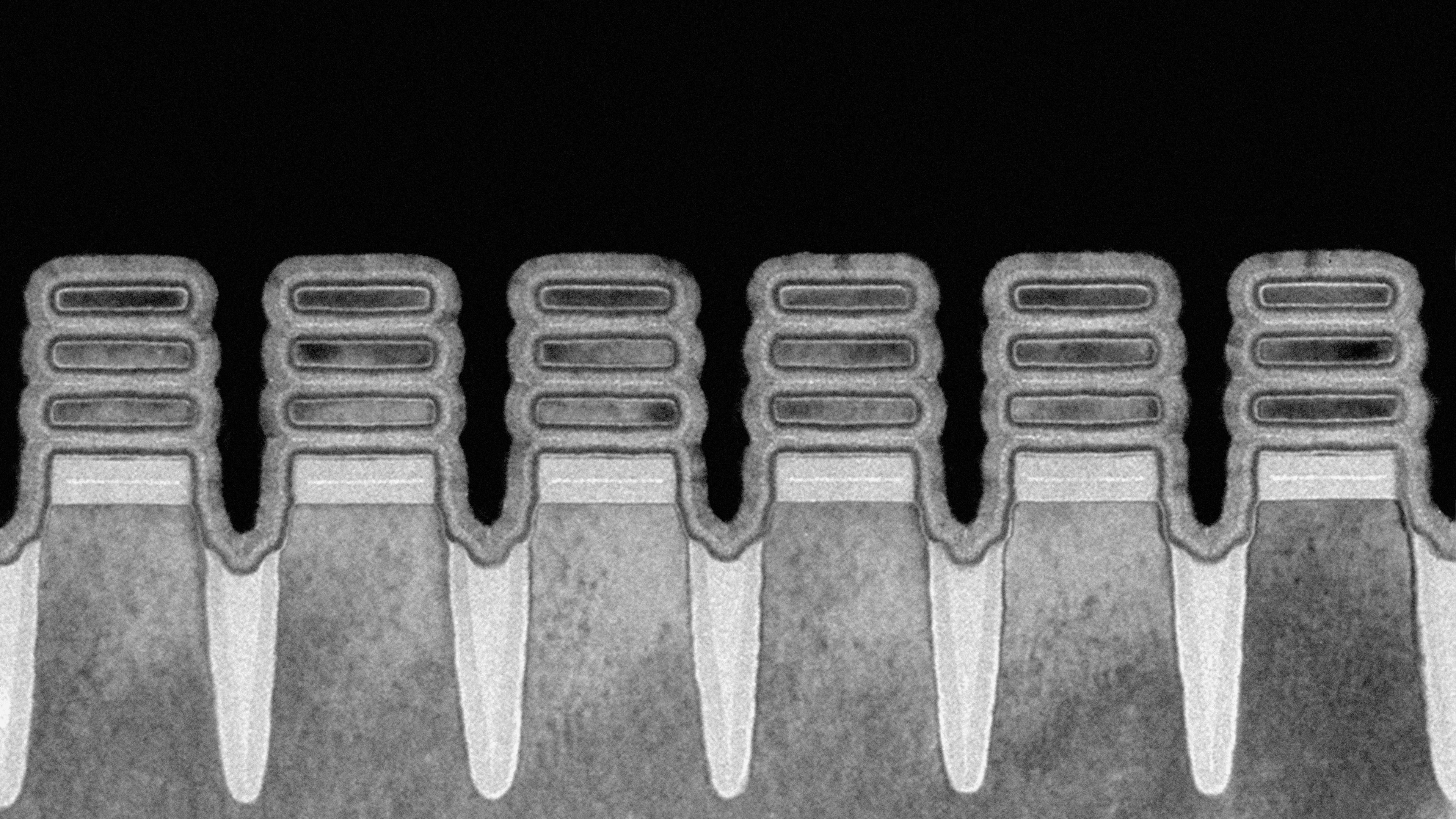
IBM Research’s second-generation nanosheet technology has paved a path to the 2 nm node, produced on a 300 mm wafer.
It seems the tech industry has forever been chasing the ideal of hardware that’s faster, cheaper, smaller and more energy efficient. Every time we come out with a more powerful chip in a smaller package, the goal posts move, and we’re looking ahead to the next iteration. Still, it’s worth pausing to reflect on the really significant milestones — how these innovations came to be and what they mean for the next generation of devices.
Today’s announcement isn’t just that our new Gate-All-Around (GAA) nanosheet device architecture enables us to fit 50 billion transistors in a space roughly the size of a fingernail. It’s not just that IBM Research’s second-generation nanosheet technology has paved a path to the 2-nanometer (nm) node. Or that we produced this breakthrough technology on a 300 millimeter (mm) wafer built at IBM Research’s semiconductor research facility in Albany, NY.
It’s all of those things, of course. But our demonstration of a nanosheet transistor for the 2 nm chip node is also a validation of several smaller milestones that proved to us this could be done, and of the hard work and dedication of IBM’s interdisciplinary team of experts in materials, lithography, integration, devices, characterization and modeling working on the project.
We first came up with the name “Nanosheet” in the summer of 2012 to describe the new device architecture we were working on at the time. The idea was to develop a sheet structure, as opposed to the nanowire structure we had been using. That was an “Aha!” moment, in that we believed the newly christened nanosheet architecture would be able to offer nanowire’s electrostatic benefits as well as the density needed to improve performance. Only through that combination of features could IBM Research deliver a transistor architecture superior to FinFET, the dominant transistor structure at the time.
This second iteration of our nanosheet transistor architecture involves a new type of horizontally stacked GAA chip design. Four “gates” on a transistor enable superior electrical signals to pass through and between other transistors on a chip.
Another “Aha!” moment on the path to 2 nm came in 2017, the year we introduced nanosheet, when we realized an inner spacer module in the transistor architecture could be a key enabler of nanosheet performance by reducing gate to source/drain capacitance. Inner spacers are critical structural elements because they define the effective gate length of GAA devices. In 2019, the team developed a new inner spacer process in collaboration with partner companies using a dry indent technique. This allows to achieve sub-1 nm process control along with improved inner spacer profile.
By combining this new dry inner spacer process with the industry’s first bottom dielectric isolation, we were able to create a 12 nm gate length, which is just two dozen atoms long. Some benefits of a full bottom dielectric isolation scheme are that it can reduce sub-channel leakage, provide immunity to process variation, and offer power-performance improvement.
It’s important to note that recent advances in transistor size — such as the 10 nm, 7 nm, 5 nm and, now, 2 nm nodes — refer to a specific generation of chips made using a particular type of semiconductor manufacturing process, much like 5G refers to the latest wireless standard. In this case, for example, 2 nm does not correspond to half pitch of contacted metal wires, as traditionally defined. In general, a smaller technology node produces smaller transistors, more of which can be packed onto a chip to make it faster and more energy efficient.
IBM researchers also developed for the first time nanosheet devices ranging from 15 to 70 nm in width using extreme ultraviolet (EUV) lithography patterning — which produces lines smaller than visible light — at the front-end-of-line (FEOL). FEOL is the first portion of integrated circuit fabrication, where transistors and other components are patterned in a semiconductor. We are the first research organization to talk about introducing EUV into the FEOL. IBM Research’s Albany lab features one of the most advanced EUV lithography tools in the industry. The ability to more precisely control nanosheet width greatly simplifies putting low power and high performance designs on the same chip.
Still another key advancement to highlight in the first 2 nm transistor is our development of a new multi-threshold-voltage (Multi-Vt) device offering with leakage levels spanning three orders of magnitude. That enables device manufacturers to better choose the level of performance required by the underlying chip architecture.
Put in perspective, 2 nm processors used in cell phones could quadruple the battery life of cell phones using 7 nm processor technology, such as the iPhone 11, Samsung Galaxy S10 and Google Pixel 5. Based on average use, this means the phone would only need to be charged once every four days.
Scaling to the 2 nm chip node transistor equates to an approximate 45 percent performance improvement over today’s 7 nm chips, using the same amount of power. That’s an approximate 75 percent power savings, at the same performance level. This kind of power/performance combination is essential to accelerating the development and delivery of advanced cognitive, edge and other computing platforms delivered via hybrid cloud environments, as well as encryption accelerators built to operate with quantum computers.
IBM Research continues to explore options for continued scaling to 1 nm and beyond. Breaking through such barriers is crucial to enabling IBM to continue to deliver the hardware that enterprises rely on to adopt the latest, most advanced AI and hybrid cloud technologies.
Although we’re still several years away from manufacturing of 2 nm node devices, IBM Research’s innovations feed directly into our commercial product roadmap. Our first commercialized 7 nm processor, based on IBM Research’s 2015 breakthrough, will debut later this year in IBM POWER10 processor, for example. Looking ahead, our leadership in semiconductor innovation could allow cloud providers or other large-scale datacenter operators to reduce their energy costs and carbon footprint by using fewer servers to accomplish the same amount of work.

