
AK
Armin Knoll
Research Staff Member, Physics of Nanoscale Systems
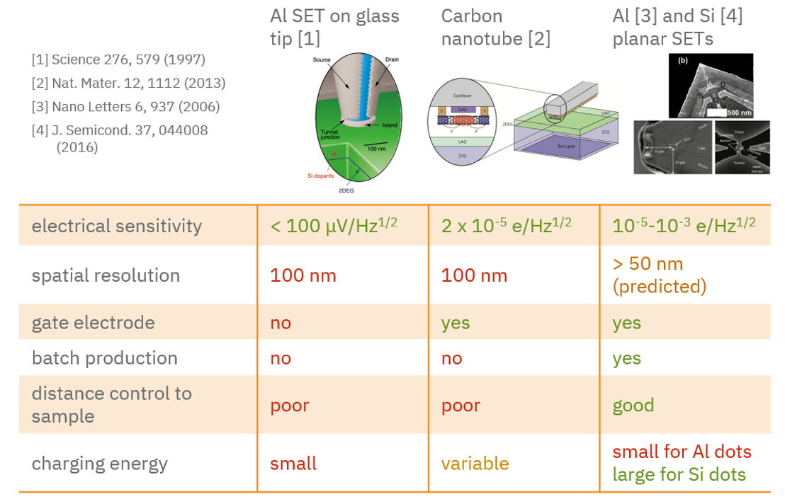
Single-electron transistors (SETs) are extremely sensitive electric field sensors capable of sensing fractions of an electron charge. Various implementations of SETs integrated onto scanning probes have been successfully used in a wide range of experiments such as imaging localized charges in semiconductors and studying nanoscale electrical transport phenomena. However, all scanning SET designs suffer from similar drawbacks: limited spatial resolution (> 100 nm), extremely low operating temperatures (< 1 K), difficult distance control to the sample under test, and challenging fabrication processes. These deficiencies greatly limit the performance and fields of application of scanning SETs.
We are using a silicon metal-oxide-semiconductor (Si-MOS) quantum dot (QD) fabricated on the tip of an atomic force microscope (AFM) cantilever as a scanning SET. The proposed geometry is expected to have improved spatial resolution, higher measurement bandwidth, and better distance control to the sample than previous scanning SETs. Additionally, the fabrication process is compatible with batch fabrication, greatly reducing the cost of the sensors.
EU FET-open project FIBsuperProbes