AI-powered satellites will upend how we observe our changing planet

Release
Mike Murphy
The U.S. Department of Commerce announced that NY CREATES’s Albany NanoTech Complex, where IBM is a key partner, will house the NSTC EUV Accelerator, a key facility that will help secure leading-edge semiconductor research, development, and manufacturing in North America.
Every industry, every supply chain, every vehicle, even our schools, cannot function without computers. Semiconductor chips are the heart of computing that enables the modern world. Over the last few decades, semiconductor manufacturing supply chain has become increasingly unbalanced and brittle. We all saw what impact that had during the pandemic. Consumers couldn’t buy things like laptops or cars, due to the lack of available semiconductor chips. Semiconductors are not only critical for the economy but are also central to U.S. national security.
This was a large part of the reason Congress passed the CHIPS and Science Act in 2022. Its aim was to ensure that the U.S. continued to lead in developing and manufacturing cutting-edge chip technologies through investments in education and research, but also through reestablishing North America as a place where the devices we rely on every day are actually built.
The CHIPS Act established the National Semiconductor Technology Center (NSTC) to create the facilities that would be responsible for rebuilding America’s advanced semiconductor supply chain. The US Commerce Department created Natcast, a division tasked with managing the NSTC consortium. Natcast first set out to identify several facilities that would be responsible for ensuring America’s leadership in advanced semiconductor technology and a balanced supply chain.
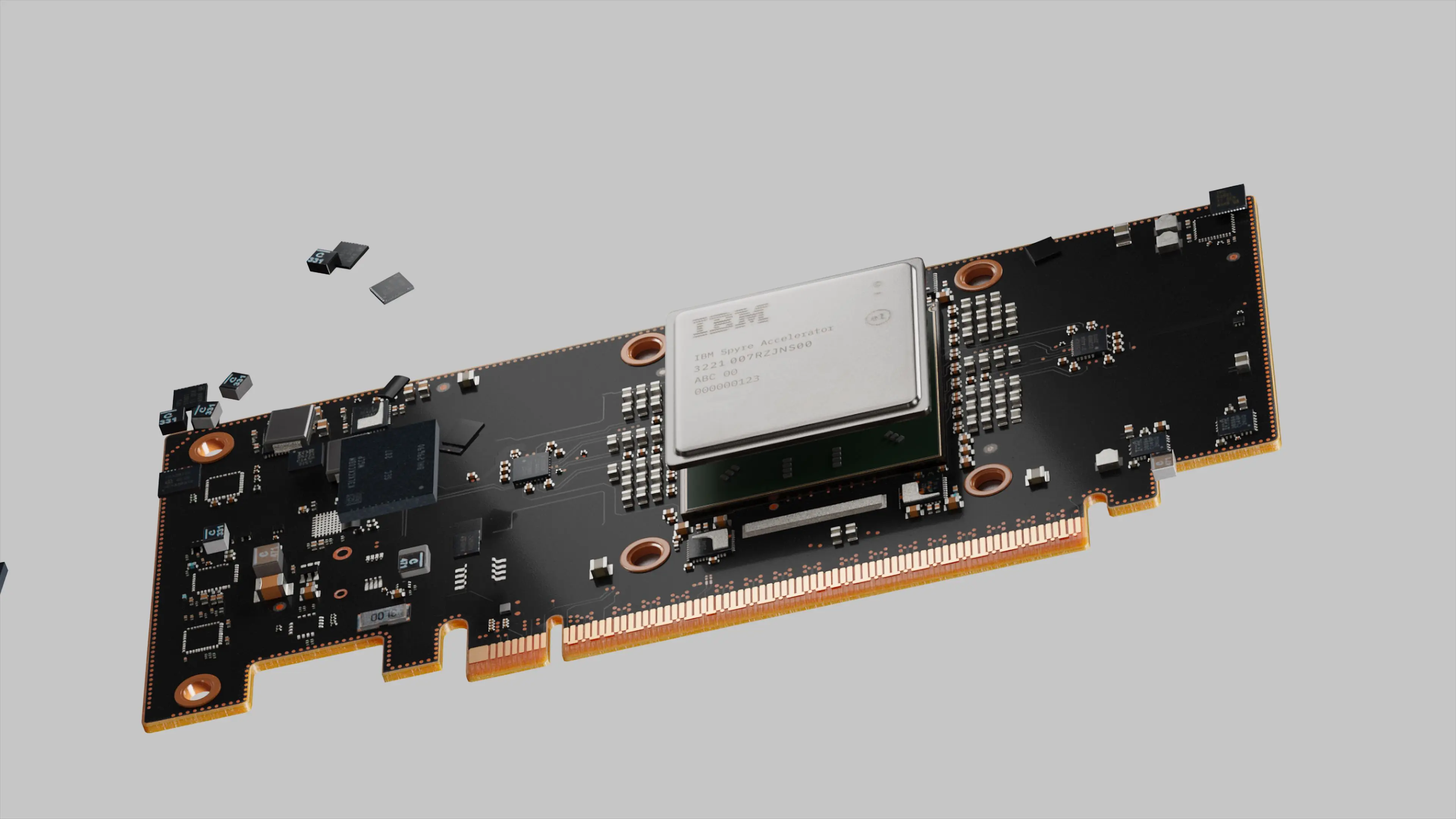
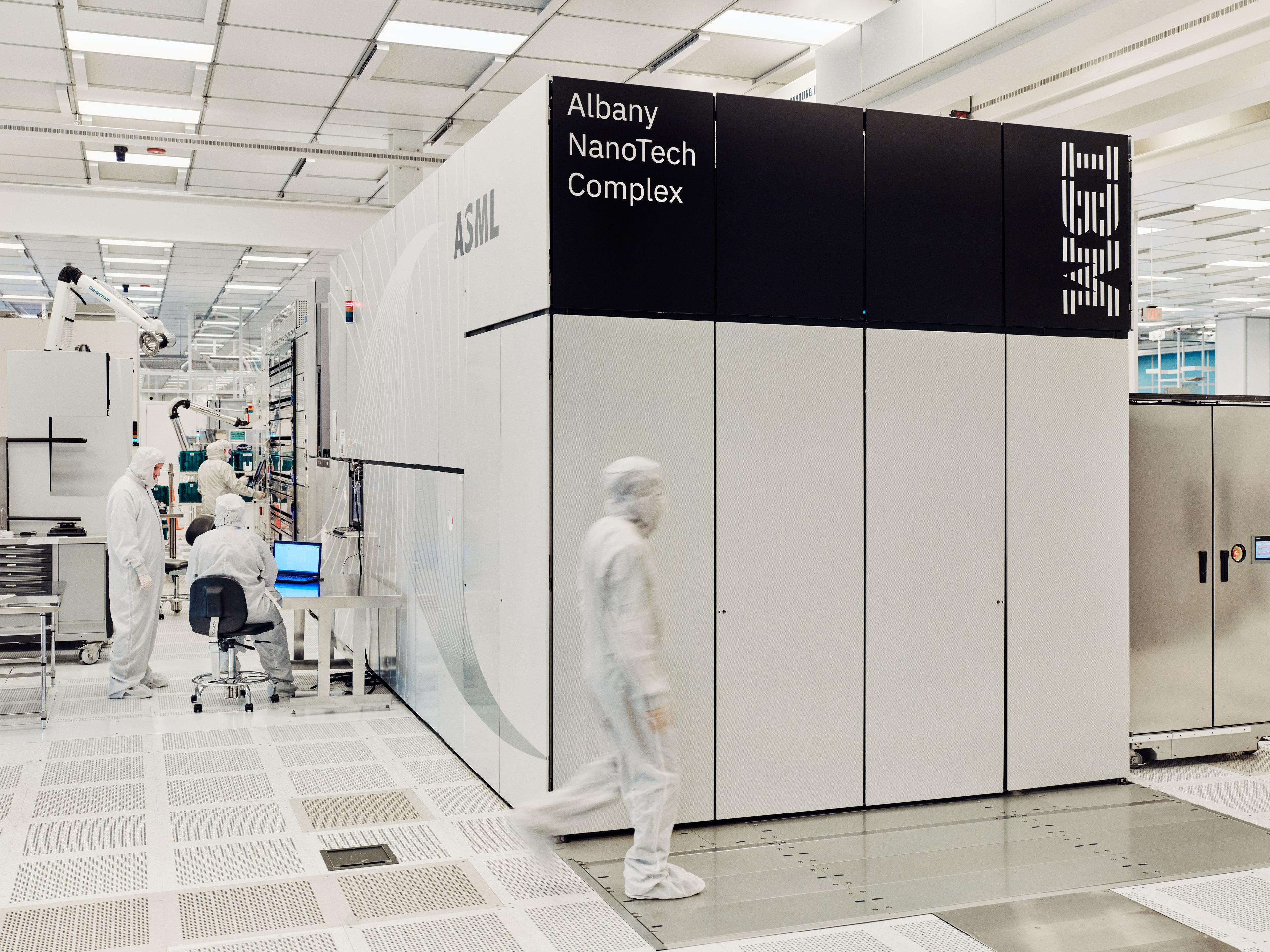
One of the essential components to the semiconductor supply chain is extreme ultraviolet (EUV) lithography. This technology mirrors centuries-old artistic techniques to print devices, with dimensions up to a few nanometers, on wafers using a very short wavelength of light generated by a specialized laser-generated plasma. Much of IBM Research’s recent breakthroughs would not have been possible without the EUV machines from the company ASML, along with the ecosystem of equipment, material, and design companies that turned ideas into reality. One of the first such EUV ecosystems started more than a decade ago at the Albany NanoTech Complex.
Natcast identified that a national EUV center would be crucial to maintaining American leadership in semiconductor research, development, and manufacturing. The other proposed centers, a design and administration facility and a prototyping and advanced packaging facility, are planned to be announced at a later date. Between the three, they will foster a strong semiconductor research, development, and production pipeline in the US.
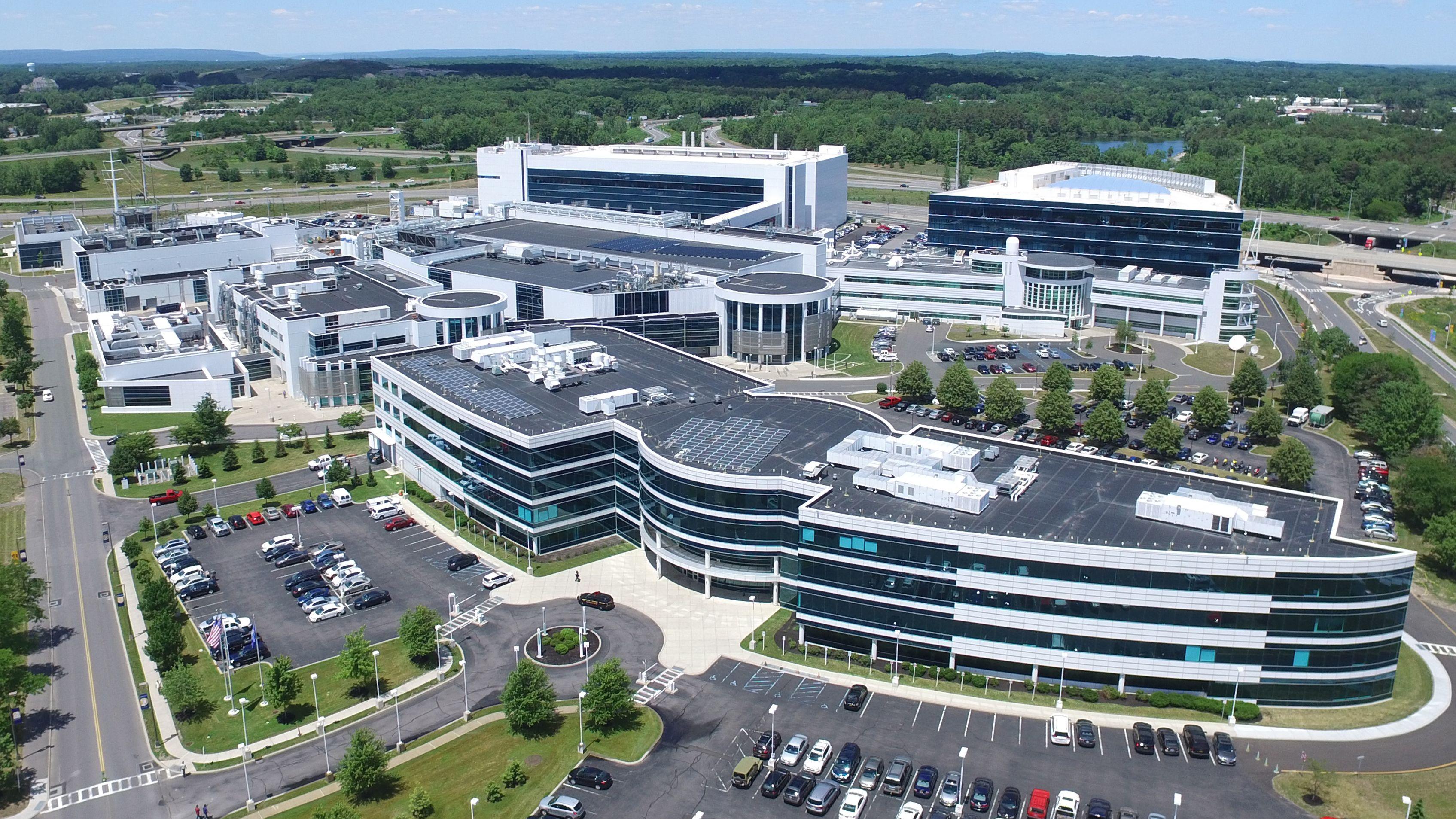
Today, Natcast announced that the new NSTC EUV Accelerator will be based at the Albany NanoTech Complex, which is owned and operated by NY CREATES, in New York state. IBM has been a key tenant at the complex for decades, and many of the company’s biggest breakthroughs in semiconductor research have taken place at the lab, including Nanosheet technology, and inventing 2nm nodes — the world’s smallest process technology for semiconductors currently being manufactured.
A decade ago, when IBM announced the world's first 7nm process technology, we said that EUV lithography would be necessary to enable that technology. Since then, it’s become the industry standard, and researchers are now looking at what comes next. To design and create the next generation of chips, ASML recently started shipping the next generation of EUV machines, called High NA (or numerical aperture) EUV, which can produce even smaller dimensions on a wafer with a high yield of usable chips.
The Albany NanoTech Complex is currently in the process of building a new research and development fabrication facility on its campus to house a High NA EUV machine, which will be the first public-private High NA EUV machine in North America. As construction continues, IBM researchers have already been working on machines at ASML’s facility in the Netherlands, and are making breakthroughs demonstrating the potential for future chip designs.
There’s around 150,000 sq ft of clean room space at Albany NanoTech, and NY CREATES is already planning to build another 50,000 sq ft in part to hold its High-NA EUV machine when it arrives. With the award of the NSTC EUV Center, NY CREATES says it should only take about three months to get operational with Natcast, and it can build even more space — up to another 100,000 sq ft — for future clean rooms as needed for the added research and development interest this will bring.
“The NSTC EUV Center will provide NSTC members with access to EUV technology to facilitate a wider range of research and a path to commercialization, including technologies with the most challenging feature sizes,” Natcast shared. "In addition to access to EUV technology, this center will also provide appropriate space for Natcast researchers and staff as well as member assignees to conduct research and collaborate in the facility.”
This is just the latest in a long string of breakthroughs and partnerships that have thrived in the upper Hudson Valley in the world of semiconductors, with IBM often at the forefront. “For 20 years, IBM and our partners at the Albany NanoTech Complex have worked together to create a thriving public-private ecosystem,” said IBM CEO Arvind Krishna. Now, with one of the most advanced semiconductor R&D facilities in North America, Albany is uniquely well positioned to support the United States in its mission to become a global semiconductor leader.