Japan
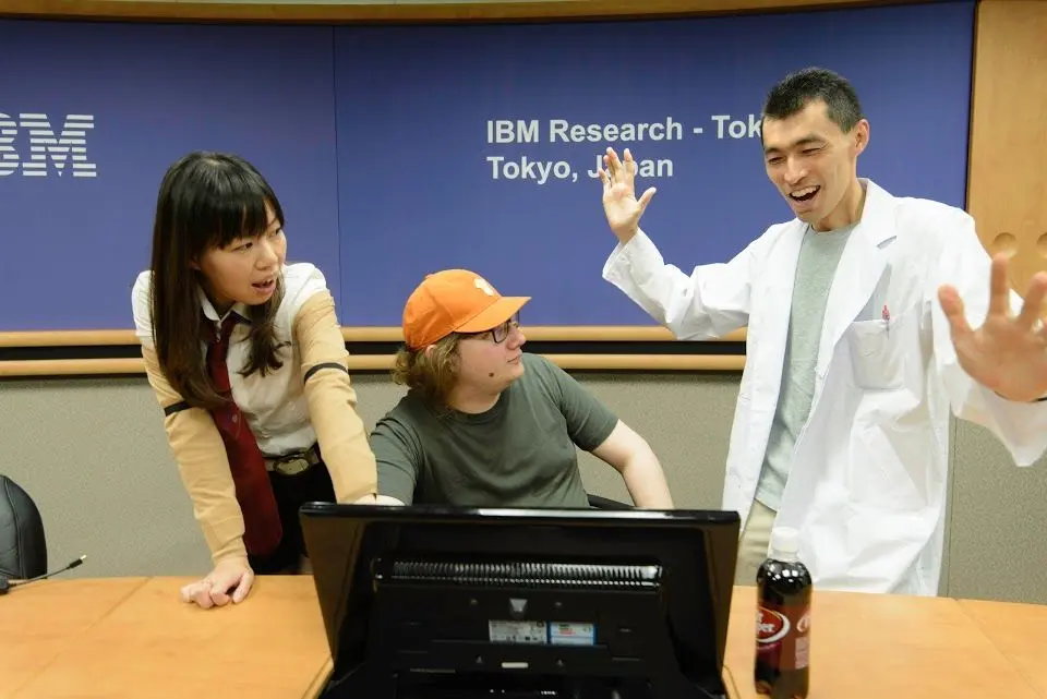
IBM Research in Japan (also known as IBM Research - Tokyo, TRL) was established in 1982 as IBM’s fourth research laboratory and the organization’s first in Asia. Located in Tokyo, Shin-Kawasaki and Kyoto, the lab led pioneering research in accessibility, microdevices, system software, embedded systems, security and privacy, and more. The lab is currently investigating new applications for foundation models and LLMs, while also leading efforts in digital health and AI-aided accessibility technologies, hybrid cloud infrastructure for AI and secure computation, quantum computing, and semiconductors.
Japanese site
Meet the team
We are a growing team of researchers, scientists, engineers, and designers pioneering scientific breakthroughs. Our work advances artificial intelligence, hybrid cloud, quantum computing, semiconductors, and scientific discovery.
Mori Ohara
Ryuki Tachibana
Gakuto Kurata
Michiharu Kudo
Shintaro (Shin) Yamamichi
Shizu Takahashi
Kiyo Kawachiya
Projects
Making Deep Neural Network systems more capable and energy-efficient.
Helping visually-impaired users to independently walk around and self-navigate
Developing a new chiplet integration technology using silicon bridge for advanced semiconductor packaging.
Multiple digital health-related applications for Alzheimer's disease using behavioral sensor data
News
Progress toward bringing quantum education to 40,000 students in Japan, Korea, and the United States
Growing the global quantum ecosystem
Think Lab
Think Lab Tokyo is an active research hub and a place for co‑creation. Through direct dialogue with IBM researchers, we provide opportunities to discover the business value of next‑generation computing and examine how it can be connected to your company’s technology strategy and implementation. Together, we explore possibilities from a practical perspective and help crystallize the next steps.
At Think Lab Tokyo, we prioritize quantum computing—the core of next‑generation computing—and hybrid cloud infrastructure for AI, which supports AI‑native business. In addition, we present research outcomes to which IBM Research – Tokyo has made significant contributions—including advanced semiconductors (such as AI chips), new applications of foundation models / large language models (LLMs), materials development platforms, and digital health and AI‑aided accessibility technologies—as concrete examples that serve as starting points for discussion.
By translating cutting‑edge technologies into practical use cases and clarifying the decision criteria needed for governance and execution, Think Lab Tokyo facilitates co‑creation workshops, fosters insight‑driven conversations, and makes the path from exploration to implementation concrete.
Location
Tokyo
Shin-kawasaki
Address
NANOBIC 7-7 Shin-Kawasaki
Saiwai-ku, Kawasaki
Kanagawa
212-0032 Japan
Kyoto
Address
Kyoto Research Park, Bldg #1
134 Chudoji Minami-machi, Shimogyo-ku
Kyoto City, Kyoto 600-8813, Japan
Join our team
We’re always looking for people excited to make a difference. See our open internship and other positions and help us invent what’s next.
